 ReLaEx
 PCB LAYOUT SERVICES
Outsource your PCB layout.
We take on board geometry, placement and routing for your assembly, directly in your ECAD tool, to your design rules and with a four-eyes review before handover.
WHAT WE TAKE ON
From schematic to a manufacturable layout.
You provide the schematic, mechanical constraints and your design rules. We develop the layout and consider electrical function, available space and manufacturing from the start.
- Board outline and geometry for existing or new enclosures
- Placement and routing to your design rules and manufacturing specs
- Positioning of connectors, interfaces and mounting points
- Missing library data added as agreed
- Layout and manufacturing data for ordering the boards
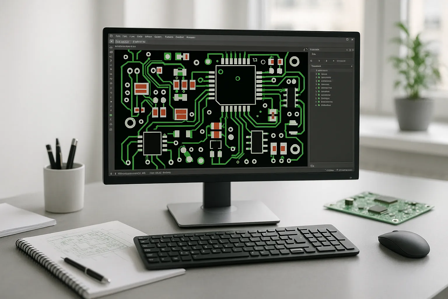
THE WHOLE PICTURE
More than placement and routing.
Florian Hocher specialises in PCB layout and demanding board geometries, David Malczewski in hardware and circuit design. That keeps layout and schematic connected.
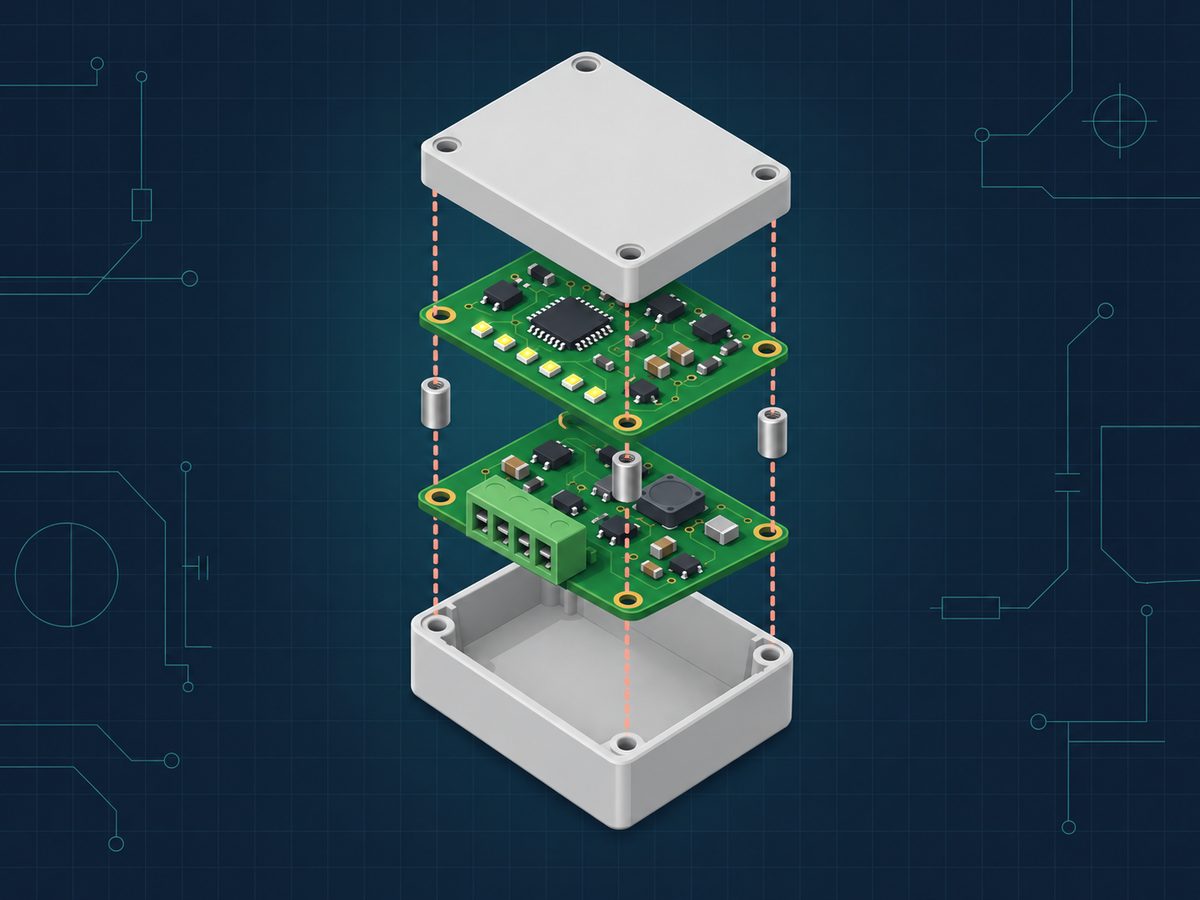
PROJECT EXAMPLE
A new layout for a device family.
Building automation devices had to fit smaller enclosures and become more economical to produce. Based on the existing schematic, we developed a new layout with stacked boards, directly in the customer's ECAD system. The result: a production-ready layout, followed by three consecutive orders.
PROJECT PROCESS
How a layout
project runs.
- 01Understand
Agree on schematic, design rules, manufacturing specs and deliverables.
- 02Align
Clarify outline, space, enclosure, interfaces and missing library data early.
- 03Implement
Placement and routing within electrical, mechanical and manufacturing constraints.
- 04Review & hand over
Four-eyes review, design rule check and 3D check, then the agreed manufacturing data.
FAQ
Questions about PCB layout.
Which ECAD software do you use?
The one you use, for example Altium Designer, Siemens PADS, KiCad, Fusion 360 or TARGET 3001!. Other tools are agreed in advance.
What do you need to get started?
Helpful are the schematic, mechanical constraints or enclosure data, your design rules and manufacturing specs, and the scope of delivery you need. Anything missing is clarified in the first conversation.
Do you work remotely?
Yes, within the European Union. On-site meetings are possible mainly in Bavaria.
Who works on my project?
The two founders, David Malczewski and Florian Hocher, themselves. We do not pass engineering work on to unknown subcontractors.
Layout support
for your project.
Briefly describe your assembly, its current state and the scope you have in mind. Together we will work out how ReLaEx can support you.
Request a projectOr email us directly: florian.hocher@relaex-engineers.com · david.malczewski@relaex-engineers.com